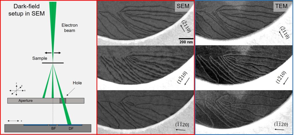
The classical way to study defects in crystalline materials is transmission electron microscopy (TEM). But do we always need this expensive and sophisticated instrument? IMN scientists have now demonstrated that the much more widespread and affordable scanning electron microscope (SEM) can be equally used when applied in scanning transmission mode (STEM) and has even advantages when it comes to defects in ultrathin 2D materials such as graphene. They transferred the well-known dark field technique from TEM to SEM thus allowing to image defects under well-defined diffraction conditions. To achieve this, the scientist inserted an aperture between the sample and the detector (as in the TEM) allowing the selection of a Bragg reflection of choice for imaging. They used their previously established low-energy nanodiffraction (LEND) setup to visualize the diffraction pattern and select the reflection.
The particular challenge with 2D materials is that no “two-beam condition” can be established due to finite size effects associated with extensive streaking of reciprocal lattice points perpendicular to the sample plane. As a result, multiple reflections are always excited, regardless of the orientation of the sample. This makes it impossible to characterize defects in bright field mode, which not only has extremely low contrast but is also severely affected by multiple diffracted beams. In contrast, dark field imaging with defined reflections is well suited for defect characterization as it shows strong contrast that is almost exclusively governed by scattering from the direct beam, thus probing a two-beam condition. Due to the lower energy of the electrons in SEM compared to TEM, electron scattering is significantly stronger resulting in higher dark-field intensities for imaging. This is particularly useful for in situ experiments where high frame rates are required for time resolution.
The IMN researchers demonstrate the feasibility of their aperture-based dark field technique for SEM instruments by characterizing basal plane dislocations in bilayer graphene, a class of defects which have attracted considerable research interest due to their exceptional structural and electronic properties. By direct comparison of results obtained on identical dislocations by the established TEM method and by the new aperture-based dark-field STEM method in SEM (see figure) they could show that the contrast is very similar in the two modes and that a reliable defect characterization in SEM is feasible, including determination of the Burgers vectors via the well-known g.b=0 invisibility criterion.
The work by Peter Denninger, Peter Schweizer and Erdmann Spiecker, entitled “Characterization of extended defects in 2D materials using aperture-based dark-field STEM in SEM”, has recently been published in the special issue of Micron dedicated to the 5th SALVE symposium and the 70th birthday of esteemed colleague Ute Kaiser, entitled “Low-dimensional materials and electron microscopy”. Congratulations to Peter and colleagues for this excellent piece of research!
Link to the paper: https://doi.org/10.1016/j.micron.2024.103703